
- 非IC关键词
深圳市广辉电子有限公司
- 卖家积分:
 营业执照:未审核经营模式:所在地区:广东 深圳企业网站:
http://www.liveic.cn
收藏本公司 人气:4445371
企业档案
- 相关证件:
- 会员类型:
- 会员年限:18年
- 陈树辉

- 电话:13686868407
- 手机:13686868407
- 阿库IM:
- 地址:深圳市深南东路金城大厦3-10-A//柜台:深圳市华强北路新华强电子世界Q3B026室
- 传真:0755-82534577
- E-mail:659974144@qq.com
产品分类
集成电路(IC)(5)
电源IC(217)
半导体存储器(20)
二极管(146)
三极管(109)
场效应管MOSFET(205)
可控硅IGBT(58)
单片机(14)
电容器(132)
电阻器(67)
电感器(113)
电位器(75)
电源/稳压器(260)
石英晶体器件(15)
声表面器件(28)
连接器/接插件(93)
开关(255)
传感器(559)
保险丝(50)
普通电池/蓄电池/动力电池(1)
变压器(333)
变送器(4)
继电器(1212)
逆变器(3)
放大器(97)
电声元件(32)
天线(2)
光电子/光纤/激光(88)
LED(10)
PLC/可编程控制器(1)
编码器(1)
安防监控器材(3)
IT/电子产品成套件(1)
电子测量仪器(4)
电子产品制造设备(1)
仪器/仪表(67)
五金/工具(5)
其他未分类(506)

 询价
询价产品信息
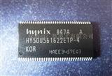
DDR SDRAM
是Double Data Rate Synchronous Dynamic Random Access Memory(双数据率同步动态随机存储器)的简称,是由VIA等公司为了与RDRAM相抗衡而提出的内存标准。DDR SDRAM是SDRAM的更新换代产品,采用2.5v工作电压,它允许在时钟脉冲的上升沿和下降沿传输数据,这样不需要提高时钟的频率就能加倍提高SDRAM的速度,并具有比SDRAM多一倍的传输速率和内存带宽,例如DDR 266与PC 133 SDRAM相比,工作频率同样是133MHz,但内存带宽达到了2.12 GB/s,比PC 133 SDRAM高一倍。目前主流的芯片组都支持DDR SDRAM,是目前常用的内存类型。
DESCRIPTION描述
The Hynix HY5DU561622ETP is a 268,435,456-bit CMOS Double Data Rate(DDR) Synchronous DRAM, ideally suited
for the point-to-point applications which requires high bandwidth.
The Hynix 16Mx16 DDR SDRAMs offer fully synchronous operations referenced to both rising and falling edges of the
clock. While all addresses and control inputs are latched on the rising edges of the CK (falling edges of the /CK), Data,
Data strobes and Write data masks inputs are sampled on both rising and falling edges of it. The data paths are inter-
nally pipelined and 2-bit prefetched to achieve very high bandwidth. All input and output voltage levels are compatible
with SSTL_2.
FEATURES特性
• 2.5V +/-5% VDD and VDDQ power supply
supports 250/200 Mhz
• 2.6V +/- 0.1V VDD/VDDQ power supply supports
300/ 275Mhz
• 2.8V +/- 0.1V VDD/ VDDQ power supply supports
350Mhz
• All inputs and outputs are compatible with SSTL_2
interface
• JEDEC standard 400mil 66pin TSOP-II with 0.65mm
pin pitch
• Fully differential clock inputs (CK, /CK) operation
• Double data rate interface
• Source synchronous - data transaction aligned to
bidirectional data strobe (DQS)
• x16 device has 2 bytewide data strobes (LDQS,
UDQS) per each x8 I/O
• Data outputs on DQS edges when read (edged DQ)
Data inputs on DQS centers when write (centered
DQ)
• Data(DQ) and Write masks(DM) latched on the both
rising and falling edges of the data strobe
• All addresses and control inputs except Data, Data
strobes and Data masks latched on the rising edges
of the clock
• Write mask byte controls by LDM and UDM
• Programmable /CAS latency 3 / 4 / 5 supported
• Programmable Burst Length 2 / 4 / 8 with both
sequential and interleave mode
• Internal 4 bank operations with single pulsed /RAS
• tRAS Lock-Out function supported
• Auto refresh and self refresh supported
• 8192 refresh cycles / 64ms
产品糸列:

结构:
